
A new light-energised material that is much brighter and more dynamic than existing photoluminescent material could power future devices fundamental to the Internet of Things.
- New material could make Internet of Things and other devices more effective, rapid and cheaper to produce
- It could be used to develop new transistor devices for fibre optic communication systems and environmental sensing
- Smart devices could process information faster, better talk to each other, make decisions, and take action with this new material.
QUT Professor Ken Ostrikov from the School of Chemistry and Physics and QUT Centre for Materials Science said the new material could be used to develop new transistor devices for electronics and photodetectors for such applications as fibre optic communication systems and environmental sensing.
“Transistors are tiny electric switches that make up computer chips that run lighting devices such as LEDs, and photodetectors, which detect light of different colours and intensities,” Professor Ostrikov said.
“These are all elements of sensing and communications devices in the Internet of Things and are the next generation of smart devices.
“The new material we have developed will enable smart devices to process information more quickly, and better talk to each other, make decisions, and take action.
“Everything from space travel to healthcare, smart cities to our homes will potentially benefit from this material.”
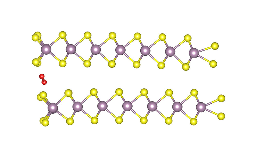
of metal sulfide called MoS2
The new semi-conducting material was developed by using plasma (ionised gas) to separate layers of atomically thin semiconductors with oxygen atoms.
“It is normally very difficult to fit oxygen molecules between the layers so we used plasma. The plasma generated electric fields to charge the oxygen molecules and then drive them to squeeze between the two layers, lifting the top layer away from the bottom one,” he said.
“When separated, the two atomic layers become electrically insulated from each other and the electrons can flow along each 2D layer without losing electrons to the neighbouring layer.
“This process resulted in new properties like strong photoluminescence and photocurrent which can be used in devices to give greater controllability and achievable currents, light doses and response speeds that are currently difficult to achieve.
“This new material could make Internet of Things and other devices more effective and rapid, and cheaper to produce.”
The research article 2D atomic crystal molecular superlattices by soft plasma intercalation was published in Nature Communications.
The collaborative project was co-led by QUT visiting researcher Professor Shaoqing Xiao from Jiangnan University and Professor Kostya (Ken) Ostrikov from the QUT School of Chemistry and Physics and QUT Centre for Materials Science.
It involved a team of researchers and students from Jiangnan university, co-mentored by professors Xiao and Ostrikov, and Professor Aijun Du from the QUT School of Chemistry and Physics and QUT Centre for Materials Science.


