Distinguished Professor Dmitri Golberg, in outlining a career spent studying materials at the atomic level, says a key moment was when he stopped using an electron microscope just to “see” and started using it as a laboratory to “do” science.
Professor Golberg, who is Co-Director of the QUT Centre for Materials Science and an ARC Laureate Fellow, will deliver the Australian Academy of Science’s Lloyd Rees Lecture in Melbourne on November 2.
In the lecture, Professor Golberg will describe the importance, and the processes, of investigating the electrical, mechanical, thermal and optoelectronic properties of materials for smart integration into modern technologies.
Professor Golberg, from the School of Chemistry and Physics in the QUT Faculty of Science, works with nanomaterials. To explain that world of nanometres to a layperson he starts with a stalwart for scale but goes further.
“Take a human hair,” Professor Golberg said. “Now slice it, along the length, maybe 50,000 times.
“So, this is the scale that we’re doing.”
Professor Golberg’s experience in nanotubes and metallic alloys has allowed him to launch a new field of nanoscale studies involving the physics, chemistry and functional properties of nanotubes filled, joined or coated with metals.
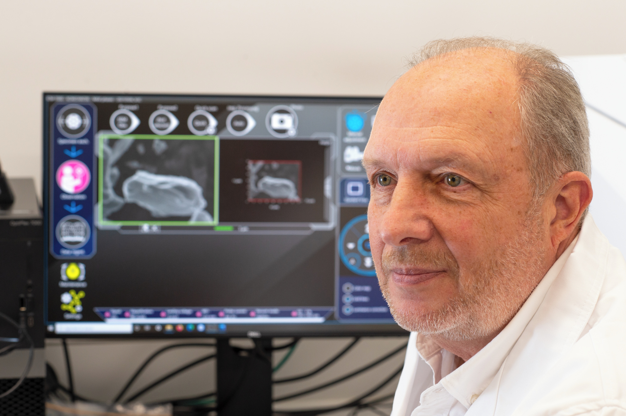
His work involves using the NeoARM Atomic Resolution Transmission Electron Microscope (TEM) at QUT, which is about 4.5m tall and housed in a specially designed building, to observe and manipulate individual atoms.
“We can zoom in up to 10 million times so, for example, a hair becomes like a soccer pitch,” Professor Golberg said.
To do experiments in that space, he has several small tools he controls within the vacuum inside of the TEM.
In some cases, there are years of research that go towards developing something on the nanoscale, such as using a tool in a TEM to create a transistor that’s 25,000 times smaller than the width of a human hair – a project, published in Science, that involved five years of work and researchers in Japan, China, Russia and Australia.
But other projects are not about building something small, but understanding the properties of material on the nanoscale to use them in new applications.
“Everything is important with respect to applications,” Professor Golberg said.
An example is carbon or boron nitride nanotubes, which have a mechanical strength 50 to 100 times greater than steel.
“Take aluminium, which is a very popular material for aircraft because it’s light. But it’s also very soft,” Professor Golberg said.
“What if you put nanotubes and reinforce the aluminium, so you have a material that is still very light but is as strong as steel?
“That’s just one application. This is not just a matter of curiosity.”
When Professor Golberg first used an electron microscope, materials were put on a flat grid and static images were taken.
“It was just observation,” he said.
“When I started, the electron microscope was just used like an eye – almost no people were studying these types of in situ tests where you can see but you can also do.”
But for the past 15 years, he has been using tools, some of which he created, to manipulate the materials, such as running a current through them or stretching them, to understand their properties. He also uses electron beams to “solder” nanomaterials together, or laser beams to act as sunlight to test materials, such as perovskites for advanced solar cells.
Before joining QUT in 2017, Professor Golberg worked at the Research Institute in Moscow for 10 years before joining the National Institute for Materials Science (NIMS) in Tsukuba, Japan, where he led the Nanotube Group for more than 20 years.
Top picture: Distinguished Professor Dmitri Golberg with the NeoARM Atomic Resolution Transmission Electron Microscope (TEM) at QUT.


