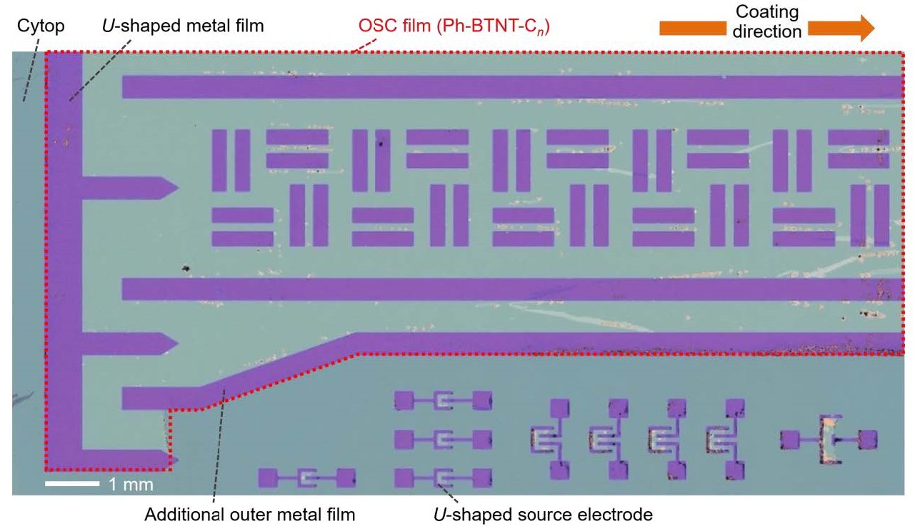
Printed organic transistors. Optical microscopy image of organic thin film transistors etched in gold. © 2020 Kitahara et al.
Researchers successfully print and demonstrate organic transistors, electronic switches, which can operate close to their theoretical speed limits. They showed high-speed operation only requires low voltages to work, which would reduce the power consumption of their applications. These kinds of transistors are used in display technology such as liquid crystal display (LCD) screens and e-ink. This is the first time this kind of transistor has been printed and it could lead to new curved, flexible and even wearable low power devices.
The chances are you are reading these words on a smartphone or computer screen. For around the last 10 years, these types of screens have been based on a display technology composed of so-called thin film transistors. These are inorganic transistors which require very little power, and they have proven themselves very capable given their widespread adoption. But they have some limits which researchers have been busy trying to overcome.
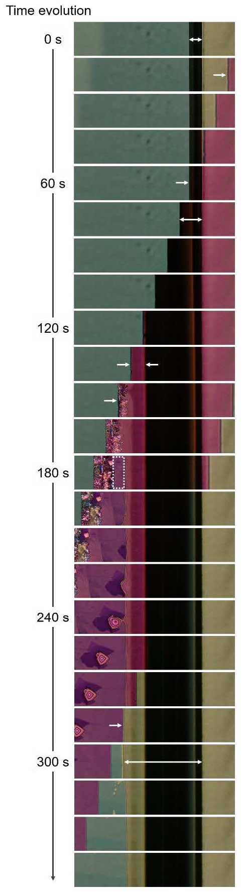
Printing organic transistors. A time series of microscope images showing the stages of printing the microscopic structures. © 2020 Kitahara et al.
“We explore new ways to improve upon thin film transistors, such as new designs or new methods of manufacture,” said Gyo Kitahara, a Ph.D. student from the Department of Applied Physics. “Organic thin film transistors, for example, have a bright future in LCD screen devices. Compared to the inorganic kind currently used, we expect the organic kind to be useful in low-cost, large-area, lightweight and wearable electronic products, especially by using printing-based production technologies.”
The idea of organic thin film transistors itself is not new, but the ability to print such devices, which would allow for a design revolution, has eluded industry and academics, until now. Professor Tatsuo Hasegawa of the Department of Applied Physics, Kitahara and their team came up with a way to print organic semiconductor films, the basis of these transistors, on a special surface that is highly solution-repellent, or lyophobic. This means ordinarily the surface would repel the materials required to print the structure of the transistor, which seems counterintuitive as to why such a surface would be useful at all. But lyophobic surfaces are responsible for creating transistor structures that are finely tuned for high performance. So how did the researchers overcome their repellent nature?
“We made use of a fluidic property you probably see every time you wash your hands with soap,” said Kitahara. “Soap bubbles can hold a shape by lowering the surface tension of liquid. We presume that the soap-film mechanism should be effective for formation of a thin liquid layer on lyophobic surfaces in spite of the repellent forces. Solid semiconductor films can be formed and grown via the formation of thin liquid layers during the printing processes.”
With this hurdle of how to print organic transistors overcome, other researchers can build on the team’s findings and find ways to scale this method up. With a proliferation of large, flexible or wearable devices, Hasegawa’s team dreams of seeing a convergence between the real world and virtual world in ways we’ve never seen before.
“After having experimented by trial and error, we eventually found that the use of a special U-shaped metal-film pattern seems to be effective for uniform film growth thanks to the way it creates a thin liquid layer on lyophobic surfaces,” said Kitahara. “We anticipated the results beforehand to some extent, but the success of these findings was finally demonstrated and obtained after overcoming several difficulties, which brought great pleasure and happiness to me.”


