A tiny new chip could give cameras and sensing systems a far sharper view of the world, helping them detect subtle differences in materials and environments that standard colour imaging systems cannot see.
In research led by Zhejiang University in collaboration with RMIT University, scientists have demonstrated a new way to build light‑analysis capability directly into imaging hardware.
Cameras are highly effective at capturing images, but applications such as machine vision, automated inspection and environmental monitoring depend on understanding different colours and wavelengths of light, not just what something looks like. That information can reveal differences in materials, surface conditions or environmental changes that appear identical to the human eye.
Until now, extracting that kind of detail has typically required separate, specialised instruments. The new study points to an alternative approach, where light analysis happens alongside imaging rather than being handled by external laboratory equipment.
Published in Nature Electronics, the work shows how the compact device could support real-world applications without bulky external equipment.
 Distinguished Professor Baohua Jia (left) and Dr Han Lin from RMIT’s Centre for Atomaterials and Nanomanufacturing with advanced nanofabrication equipment used in the study. Credit: Will Wright, RMIT University
 RMIT researchers led by Distinguished Professor Baohua Jia contributed expertise in nanomanufacturing, optical characterisation and device testing, working closely with the Zhejiang University team led by Professor Jianrong Qiu to evaluate the performance of the integrated system.
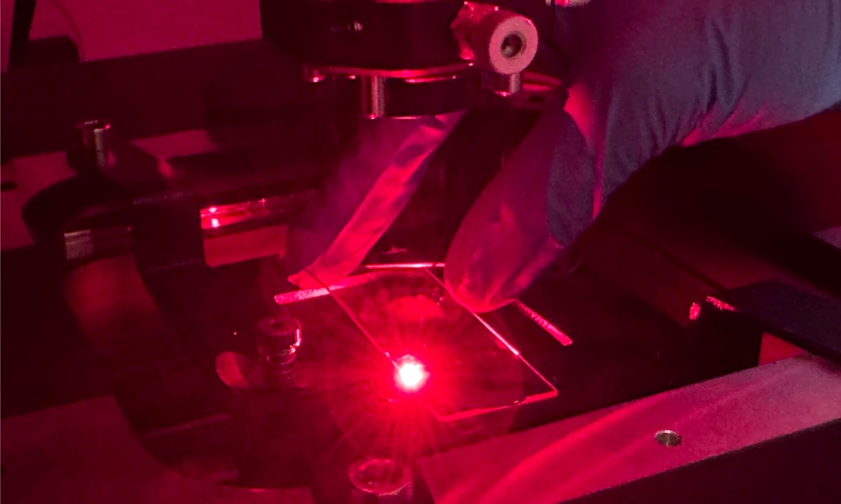
At RMIT, highly specialised nanofabrication lab equipment can build and image structures about 1,000 times smaller than a human hair in real time.
The collaboration brought together ultrafast laser fabrication and applied photonics to turn a new physical approach into a functioning prototype. Qiu, Bo Zhang and Zhuo Wang from Zhejiang University are corresponding authors of the research paper, and Dr Han Lin from RMIT University is a co-author.
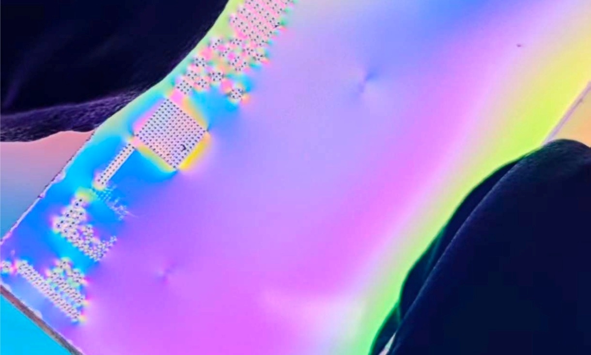 The microscale optical device developed in the study, integrated with imaging hardware to analyse light at the source. Credit: Zhejiang University
 “This is not about adding more image processing after the fact,” said Jia from RMIT’s Centre for Atomaterials and Nanomanufacturing (CAN).
“It introduces a new physical component that separates light at a very small scale, close to the sensor itself.”
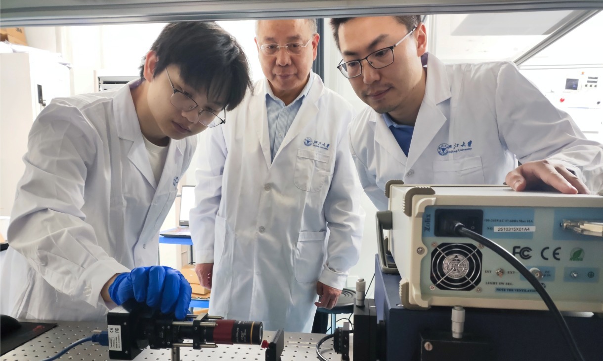 Zhejiang University researchers involved in the international collaboration on chip scale optical sensing. Credit: Zhejiang University
 How it works
The researchers used ultrafast laser pulses to create tiny spiral‑shaped structures inside transparent materials and a specialised optical system to visualise them. These structures act like microscopic light sorters, breaking incoming light into distinct patterns that a sensor can read.
In practical terms, this allows a compact device to analyse light on the spot, without moving parts or additional equipment. The approach works across visible and near‑infrared light and is largely unaffected by viewing angle, overcoming several common limitations of existing microscale technologies.
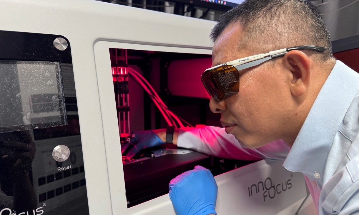 Dr Han Lin operates a nanofabrication system at RMIT, where structures around 1,000 times smaller than a human hair can be built and characterised in real time during the manufacturing process. Credit: Will Wright, RMIT University
 From concept to working prototype
To demonstrate the feasibility of the approach, the team integrated the structure with a commercial image sensor and showed that it could detect spectral information and support microscopic spectral imaging.
“Demonstrating that a concept works at the chip level is a critical step,” Lin said.
“It helps move the discussion from what is theoretically possible to what kinds of sensing systems could realistically be built in the future,” Qiu said.
 Inside a nanofabrication system at RMIT, where structures around 1,000 times smaller than a human hair can be built and characterised in real time during the manufacturing process. Credit: Will Wright, RMIT University
 The researchers say the work is still at an early stage rather than a finished product, but the work establishes a new strategy for building compact sensing tools that can go beyond simply capturing images.
“Next steps include scaling up fabrication, testing other materials and refining the software used to reconstruct light information,” Zhang said.


