
As artificial intelligence (AI) drives demand for faster data transfer, conventional silicon optical modulators face speed and energy-efficiency limitations, often requiring power-hungry electronic circuits. By designing electrical and optical structures together, researchers built signal equalization into a compact slow-light silicon modulator. The device achieved data rates of 180 Gb/s without digital signal processing equalization and 200 Gb/s using a low-complexity 11-tap digital equalizer, offering potential for high-capacity, energy-efficient optical connections in future AI data centers.
Enabling Ultrafast, Energy-Efficient Optical Communication with a Compact Slow-Light Silicon Modulator
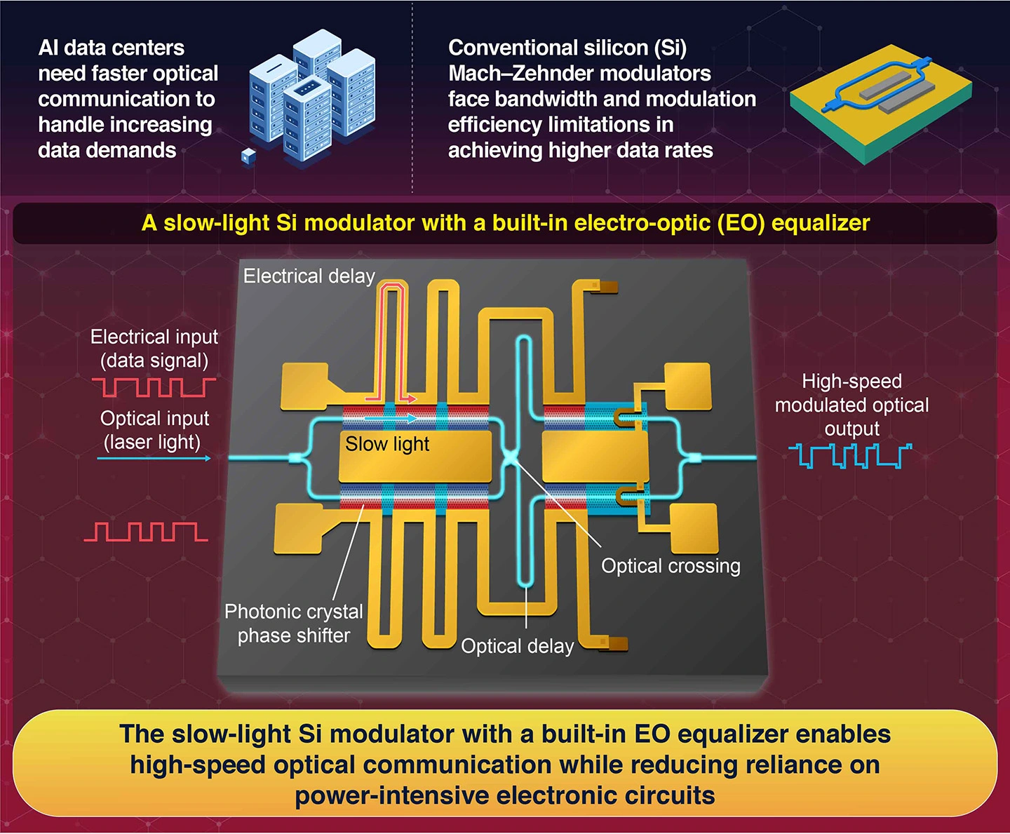
The growing capabilities of artificial intelligence (AI) are driving data centers to transfer increasingly large amounts of information between processors. Optical interconnects, which use light for data transmission, can meet this demand. However, achieving higher transmission speeds while keeping devices compact and energy-efficient remains a challenge.
Silicon (Si) Mach-Zehnder optical modulators are key components in optical interconnects, using electrical signals to encode data onto light. However, conventional designs often require long electrodes and high drive voltages, and their bandwidth can also limit transmission speeds. To compensate, communication systems often rely on complex digital signal processing (DSP), increasing the demands on electronic circuits.
Against this backdrop, a research team including Assistant Professor Keisuke Kawahara and Professor Nobuhiko Nishiyama from the Department of Electrical and Electronic Engineering, Institute of Science Tokyo, Japan, together with Professor Toshihiko Baba from Yokohama National University, Japan, and Research Team Leader Yuriko Maegami and her colleagues at the National Institute of Advanced Industrial Science and Technology (AIST), Japan, demonstrated a compact optical modulator capable of high-speed data modulation. Their study, published in Volume 17 of the journal Nature Communications on October 22, 2026, presents an approach that integrates an electro-optic (EO) equalizer directly into the device to improve bandwidth while reducing reliance on external processing.
The researchers used a photonic crystal waveguide to produce the slow-light effect in the Si modulator. A photonic crystal waveguide uses a carefully designed pattern to control how light travels through it. The slow-light effect strengthens the interaction between light and the material, allowing efficient modulation over a short distance at a low drive voltage.
However, slow-light Si modulators also face bandwidth limitations. To address this, the team divided the modulator’s phase-shifting section into segments and incorporated optical delay lines and crossings. Through electronics-photonics co-design, the team coordinated the electrical and optical responses so that the modulator itself performs part of the signal equalization.
“By integrating an EO equalizer into the slow-light modulator, we can extend its bandwidth and reduce waveform distortion,” says Kawahara.
The device was fabricated using AIST’s silicon photonics process for 300-mm wafers. The modulator’s core measured just 320 μm in length. In experiments, it achieved a data transmission rate of 180 Gb/s using pulse amplitude modulation 4-level (PAM4) without DSP equalization. PAM4 uses four signal levels, allowing each symbol to carry two bits of information. With a low-complexity digital equalizer using 11 taps, the device reached 200 Gb/s.
The team also demonstrated on-off keying (OOK), which represents data using two signal levels. At 140 Gb/s, the modulator operated with a drive energy of 26 fJ/bit (femtojoules per bit). This energy figure applies to the OOK demonstration, not the 200-Gb/s PAM4 result.
These findings could help advance optical connections for future AI data centers, where high-speed communication must operate within tight energy constraints. “I see this as a step toward rethinking how signal processing is implemented through the joint design of electronic and photonic circuits,” says Kawahara.
Further work is needed before the technology can be used in practical systems. In particular, reducing optical insertion loss will be important for applications such as co-packaged optics, which bring optical and electronic components closer together. With continued improvements, the design could contribute to compact, high-capacity optical links for next-generation data centers.
This work was supported by JSPS KAKENHI, NEDO, and Lumentum Japan Inc. Keysight Technologies provided equipment on loan for the experiments.
Reference
- Authors:
- Keisuke Kawahara1,2, Tai Tsuchizawa3, Noritsugu Yamamoto3, Yuriko Maegami3, Koji Yamada3, Nobuhiko Nishiyama1,4, and Toshihiko Baba2,5
- Title:
- Reduced-DSP 200G/λ low-voltage slow-light silicon modulator enabled by built-in EO equalizer
- Journal:
- Nature Communications
- Affiliations:
- 1Department of Electrical and Electronic Engineering, Institute of Science Tokyo, Japan
2Department of Electrical and Computer Engineering, Yokohama National University, Japan
3National Institute of Advanced Industrial Science and Technology (AIST), Japan
4Photonics Electronics Technology Research Association (PETRA), Japan
5Institute of Advanced Sciences (IAS), Institute of Multidisciplinary Sciences (IMS), Yokohama National University, Japan