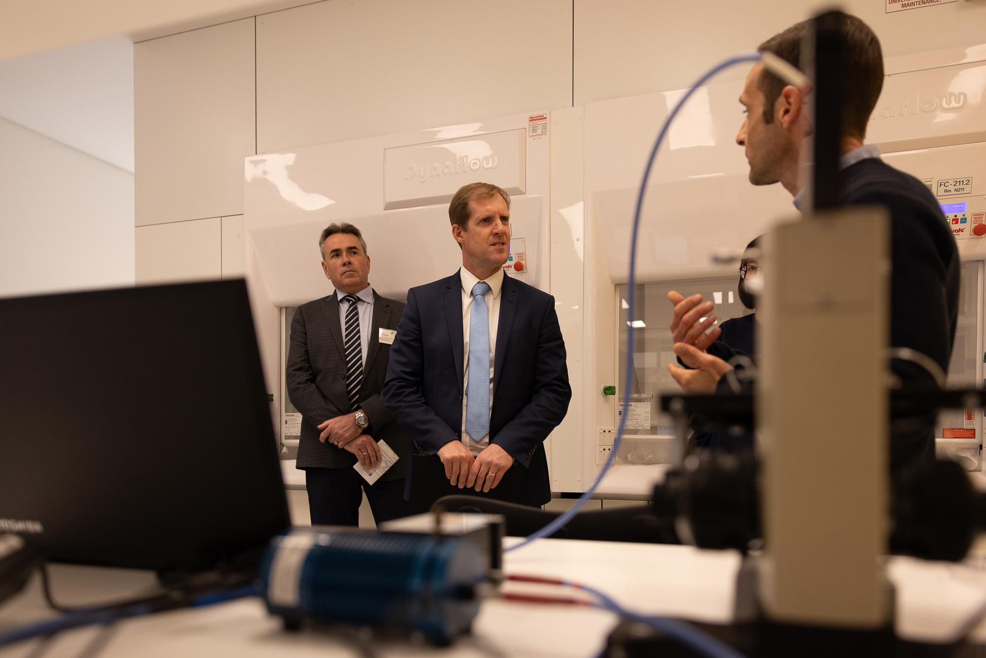
Trade and Investment Minister Stephen Patterson meeting students in the University of Adelaide’s new Advanced Materials Facility.
Advanced materials research and design, including revolutionary new technology with potential for sterilising surfaces against COVID-19, is taking a step forward with two new facilities at the University of Adelaide.
“The University of Adelaide’s Advanced Materials Facility and Silanna’s QuFab facility are set to push the boundaries of advanced materials research, design and fabrication,” says the University of Adelaide’s Acting Vice-Chancellor Professor John Williams.
“By having industry and businesses such as Silanna on our campuses we are changing the very culture and nature of our campuses.
“Silanna’s expertise links into many different cutting-edge areas across the University including advanced materials research and teaching in our new facility.”
“These labs are where the future minds of the advanced materials industry will be trained.”Professor David Lewis
Advanced materials are made by modifying existing materials or creating new ones so that they have superior performance. They can be structural and functional, inorganic, organic or a hybrid of these, and can be soft or hard depending on their characteristics. These materials will make homes, vehicles and gadgets more energy efficient and environmentally friendly.
QuFab and the Advanced Materials Facility are both located on North Terrace campus in the University’s Faculty of Engineering, Computer and Mathematical Sciences.
“Today’s undergraduates and postgraduates will undertake their studies in the Advanced Materials Facility at the same time as having the unparalleled opportunity to tap into the minds of the experts working at QuFab,” says the University of Adelaide’s Professor David Lewis who is the Head of the School of Chemical Engineering and Advanced Materials.
“Our students will have access to a diverse range of facilities in which they will discover the world of advanced materials through engineering research, educational teaching and training activities, with a strong focus on new materials for energy, catalysis and semi-conductors.”
“These labs are where the future minds of the advanced materials industry will be trained.
“In the same way that the brightest minds will be attracted to study here, some of the world’s top research talent in this area is also being attracted to work here.”
Silanna Chief Scientist Dr Petar Atanackovic is focusing on designing and making prototypes of the next generation of semi-conductors at QuFab.
“At QuFab here in Adelaide, we are designing and manufacturing atomically engineered crystalline semiconductors using applied quantum mechanics and proprietary atomic layer deposition technologies. These new compositions of matter are then fabricated into electronic and optoelectronic devices for applications including power conversion and extreme ultraviolet light detectors and emitters – we are unlocking new technology areas of fundamental physics, chemistry, electronics and photonics,” Dr Atanackovic says.
“Silanna’s UV-C light emitting diode (LED) technology is already commercialised and the work here at QuFAB is building the next generation of improved materials and technology. To achieve these goals we need talented and highly skilled people and it is one of the main reasons we have embedded ourselves into the University of Adelaide.
“Fortuitously, these UVC devices may be used to deactivate surfaces contaminated by COVID-19 and are already being used to sterilise air, water and surfaces by virtue of UVC interacting advantageously with an organism’s DNA.”
Dr Atanackovic studied at the University of Adelaide and pursued a career in Silicon Valley before returning to Adelaide.
“I wanted to try and create some of the unique opportunities given to me while at Stanford University and Silicon Valley and bring them here to Adelaide. A whole ecosystem is beginning to appear, not only with large infrastructure investment like QuFAB, but also having the support of the University in building an environment for knowledge creation in this new area of quantum engineering,” he says.
In 2018 global semiconductor sales were worth $490 billion in total of which the diode, laser and LED segment of the market was worth $38 billion.
“The QuFab facility and the Advanced Materials facility, located here at the University of Adelaide, demonstrate how South Australia is investing in the future,” says Trade and Investment Minister Stephen Patterson.
“Innovation, global connectivity, hi-tech research and design into this cutting-edge technology, will have a snowball effect.
“South Australia’s hi-tech sector is gaining a worldwide reputation and partnerships like this enable our state to have the rare ability to rapidly scale to meet the skilled workforce needs of global technology companies.
“The investment in research, design and education here and now, will have far reaching and long-term benefits for our economy and society.”


