Electron microscopy is built on a bitter irony: The process of beaming electrons allows scientists to peer into the atomic structure of biomolecules and materials, but the electrons can also damage their target.
“I can only deliver so many electrons before I fry the sample, but I need a certain number of electrons before I can see the things that I need to see,” said David Muller, the Samuel B. Eckert Professor of Engineering in the Department of Applied and Engineering Physics. “Otherwise, everything’s just lost in this speckly noise. So there’s a trade-off.”
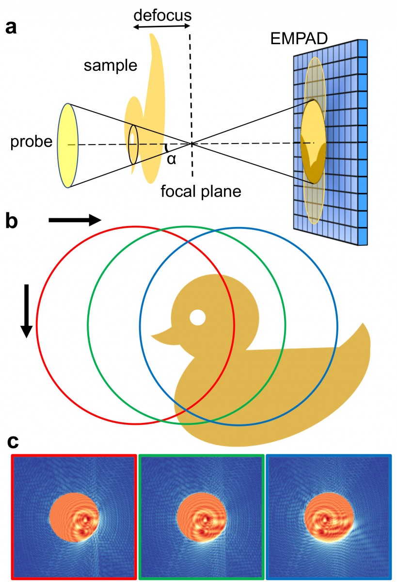
In order to perform faster, more precise electron imaging, researchers overlapped two sheets of atomically thin materials – a single layer of tungsten disulfide atop a single sheet of molybdenum diselenide. By slightly angling one layer’s atoms, a complicated moiré pattern is created, giving the researchers a wider range to image.
In 2017, Muller co-led a collaboration with Sol Gruner, the John L. Wetherill Professor of Physics, on a high-powered detector that, in combination with a technique called ptychography, set a world record for nanoscale resolution, measuring down to 0.39 ångströms or 0.039 nanometers; a nanometer is one-billionth of a meter.
Now, Muller’s research group has gone a step further by developing a new form of ptychography that uses complex algorithms to achieve faster, more efficient imaging with picometer (one-trillionth of a meter) precision that won’t damage samples so easily.
Muller’s team encountered an additional irony when they realized they obtained the best results by defocusing their detector and blurring the beam.
“It’s a little counterintuitive. Normally the best conditions for taking an image would be a really well focused beam on the smallest spot you could get,” said Muller. “But our approach, going out of focus, works because our algorithm lets us recover the shape of the blur. It gave us a lot more information to work with.”
The result, Muller said, is “hardware to count every electron and software to make sure every electron counts.”
The team’s paper, “Mixed-State Electron Ptychography Enables Sub-Angstrom Resolution Imaging with Picometer Precision at Low Dose,” published June 12 in Nature Communications. Postdoctoral researcher Zhen Chen is the paper’s lead author.
In conventional imaging, only a small fraction of the transmitted electrons are recorded. In fact, if all electrons were collected at every point, there would be no image contrast. Ptychography, on the other hand, is able to use every electron by scanning overlapping scattering patterns of a material sample and reconstructing the data into an ultraprecise image, although it requires a much more sophisticated detector, such as the EMPAD that Muller and Gruner developed.
“This time, we bit the bullet and decided we’re going to deal with all of this stuff properly, because computers are more powerful, and the algorithms are a lot more intelligent,” said Muller, who co-directs the Kavli Institute at Cornell for Nanoscale Science and co-chairs the Nanoscale Science and Microsystems Engineering (NEXT Nano) Task Force, part of Cornell’s Radical Collaboration initiative. “With increased computational power, we’re able to deal with all the things that you need to deal with to get a good image.”
In order to get their out-of-focus method to work, Muller’s team took an unorthodox approach. Rather than assuming the electrons were in pure quantum states, which are easier to model for imaging, the researchers focused on superposing mixed-state electrons – i.e., a linear combination of pure electron wave functions. This allowed the team to capture the fine-grained contrast buried in an image’s “speckly noise.”
“If you take a laser pointer and you shine it on a wall, you’ll see lots of lovely speckle. Now if you took an LED or a flashlight, you wouldn’t see any of that speckle. The reason the laser has a speckle is because it’s a very pure state, and that speckle is washed out when I use an LED or a flashlight,” Muller said. “Normally, if my source isn’t perfect, I lose the speckle, and therefore I lose a lot of information. Our process says, well, this thing is actually made up of different wavelengths and if you account for each wave separately, you can find there really is speckle on each one of those.”
The researchers scanned a monolayer of tungsten disulfide atop another single-layer sheet of molybdenum diselenide. By slightly angling one layer’s atoms, a complicated moiré pattern emerges between the crystals, giving the researchers a wider range to image. Whereas previously they would have imaged one atom at a time, ptychography allows them to image approximately 100 by 100 atoms in parallel series and overlap the snapshots together.
Using this method, the researchers were able to record data four times faster at double the resolution. Mixed-state ptychography also gives scientists the option of imaging fragile materials at a lower resolution, with far fewer electrons than previously required – an electron dose could be reduced by a factor of 50. This could be particularly helpful for imaging biological molecular structures and battery materials that are easily damaged by high intensities of energy, Muller said.
Co-authors include Yi Jiang, Ph.D. ’18; Yimo Han, Ph.D ’18; and researchers from the Paul Scherrer Institut, King Abdullah University of Science and Technology, and Chang-Gung University.
The research was supported by the Platform for the Accelerated Realization, Analysis and Discovery of Interface Materials (PARADIM), a National Science Foundation-supported platform. It made use of the Cornell Center for Materials Research, which is supported by the NSF’s Materials Research Science and Engineering Center program.


