Key Points
- Australian and international researchers have developed advanced microelectronics that are resistant to the harsh radiation in space and other environments
- The microelectronics were tested at ANSTO’s Centre for Accelerator Science, where a high energy microprobe technology can simulate the effects of space radiation
- ANSTO has a range of specialist facilities to support space research and the space industry in Australia
A team of Melbourne researchers and international partners from the Italian Instituto Nazionale de Fisica Nucleare (INFN) and CERN, who are developing radiation-hardened semiconductor chips, used the unique state-of-art high-energy ion microprobe on the SIRIUS ion accelerator at ANSTO’s Centre for Accelerator Science to test a prototype.
The SRAM chip was built on a nanoscale CMOS technology for use in space, and high energy accelerator or nuclear facilities where operating control systems are exposed to radiation.
“> Play
Play
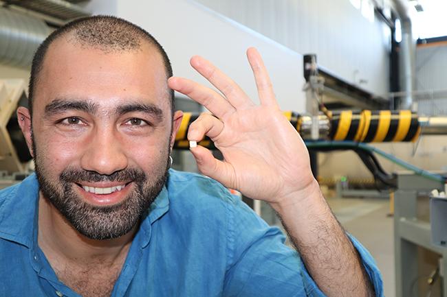
A team led by scientist Dr Jafar Shojaii, Senior Research Fellow at Swinburne University, Honorary Fellow at the University of Melbourne and with partners from INFN and the University of Milan, designed a prototype SRAM memory chip with a new architecture using an original approach to eliminate single event upsets (SEUs) and single event effects (SEEs) to boost its operating reliability in radiation hard environments.
The team together with Centre partners used the SIRIUS microprobe to simulate the exposure of selected parts of the prototype chip using a beam of ions and protons in a vacuum.
High energy protons are the most abundant particle type radiation in Lower Earth Orbits and high energy heavy ions like carbon are generated as secondary recoiled particles.
“The novelty of testing at the Centre for Accelerator Science is that the nuclear microprobe enables high-precision irradiation with sub-micrometre accuracy by means of computer-controlled rapid scanning,” said Dr Shojaii.
“This mode of irradiation testing allows us to investigate a SEE in a selected chip circuitry while ensuring other vital chip parts that remain intact.”
The SIRIUS microprobe system can generate and focus a large variety of ion beams and allows a user to select a linear energy deposition rate in a preselected region of the chip at a penetration depth.
Radiation can produce parasitic signals or damage crucial electronic components of operating control systems, such as memory and processing chips, which are used in space satellites, instruments and vehicles.
“The impact of radiation damage to the performance of the newest generations of microelectronic technologies is still not very well understood in the scientific community,” explained Dr Shojaii.
“Only an experiment can confirm that the performance of the technology will not be adversely impacted by radiation,” he said.

“We need to validate that the hundreds of millions of transistors in a single chip will perform suitably at the device level, before use in space. The radiation effects on semiconductor chips have been one of the main reasons for satellite failures in space missions,” said Dr Shojaii.
“Our program is greatly supported by the Department of Defence, as this novel capability is extremely important in defence applications.”
The chip prototype was selectively irradiated using the SIRIUS nuclear microprobe. The modular experimental end-station was customised to meet the user demand of chip radiation testing during its normal operation.
Nanoscale, ultra-low energy electronics are a practical choice for space where the weight and the low energy consumption combined with the fast performance is important. However, this technology is extremely sensitive to the effects of high energy and high penetration radiation.
The custom chip was tested under different laboratory conditions, such as different particle mass and energy, increasing particle rate and increasing accumulated dose, over the course of three experiments performed at ANSTO in the last 12 months.
An absorbed radiation dose by an electronic component is usually expressed in Rads.
The new chip architecture proved to be radiation hard for threshold doses required by a space community (100s of kRads) and particle rates up to 10 MHz.
Moreover, the chip was able to withstand very high doses up to 100 MRad range, which is required by the high energy accelerator community, such as the Large Hadron Collider experiment at CERN in Switzerland.
“The Sirius accelerator system coupled to multiple instrument beamlines is one of ANSTO’s and Australia’s flagship research facilities for applied science, and it is well-suited for the characterisation and testing of materials in radiation hard environments,” said Dr Pastuovic, a senior accelerator scientist at ANSTO’s Centre for Accelerator Science, who specialises in applications for advanced materials and device technologies.
“Precision irradiation is used on advanced material and device prototypes in testing for space, health, biology, electronics, communication, energy and quantum science. It is quickly becoming one of the Centre’s core capabilities,” said Dr Stefania Perracchi, an accelerator beamline scientist at the Centre for Accelerator Science, who specialises in radiation dosimetry and also collaborated on the experiments
“The ability of expert staff to model and prepare experiments, fabricate and customise technology on-site in real-time is indispensable in complex measurements for high-tech R&D,” said Dr Pastuovic.
“The initial contact with Dr Shojaii was made by former staff member Adam Sarbutt surreptitiously and we are grateful for his initiative,” said Dr Pastuovic.


