What the research is about
Even dishes that taste alike can be made with different ingredients and seasoning combinations. Just as it is difficult to identify the exact recipe from taste alone, in manufacturing it can be challenging to work backward from a single measurement and determine what is happening inside a material.
Semiconductors used in smartphone and television displays are a good example. Two devices may show almost identical electrical behavior even though the number of defects in the material and the ease with which electrons can move through it are different. This makes it difficult to infer the material’s internal state from measurements alone.
Conventionally, researchers would begin by assuming a possible internal state, test it through calculations, change the assumption if the result did not match the measurements, and then try again. Reaching even one plausible answer often took several days. In recent years, researchers have therefore explored using machine learning to speed up this process.
However, AI cannot solve this kind of problem easily. A single measurement may be explained by several different internal states of the material. When one problem has multiple possible answers, an AI model can struggle to learn how to connect the observed result with its underlying cause. As a result, conventional machine-learning methods have struggled to analyze a broad range of devices with widely varying defect levels and electron mobility.
Why this matters
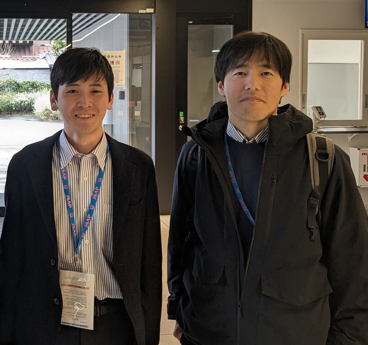
To overcome the challenge of multiple possible answers, a research team at Institute of Science Tokyo (Science Tokyo), including Assistant Professor Keisuke Ide, Masatoshi Kimura, who was a graduate student at the time, and Professor Toshio Kamiya, developed a new framework using a tandem neural network consisting of two lined networks.
The first network estimates the internal state of the material from measurement data. The second then checks whether that estimated state can reproduce the original measurements. In simple terms, one AI proposes a possible cause, while the other checks whether that explanation can truly account for the observed behavior.
Using this approach, the researchers accurately estimated several numerical values describing the material state of semiconductors with widely varying defect levels and electron mobility. The analysis took less than one millisecond. Because conventional analysis could require several days to reach a solution, this represents a dramatic reduction in processing time.
The team also tested the method on semiconductor devices that they had fabricated. Using only the values estimated by the AI, they were able to closely reproduce the actual measurement results.
The model also maintained high accuracy with only about 400 training examples-roughly one-hundredth of the number used in previous studies. Because generating training data also takes time, maintaining high accuracy with such a small dataset is an important advantage for practical use.
What’s next
With further development, this technology could make it possible to rapidly analyze large amounts of measurement data in semiconductor factories and detect changes in manufacturing conditions or material states in real time. It could also contribute to digital twins, which virtually reproduce manufacturing processes on computers, and autonomous experimentation systems in which AI automatically conducts and analyzes experiments.
Problems in which a single result may have several possible causes also arise in materials science, chemistry, optics, and many other fields. The method developed in this study could therefore provide a broadly useful way to tackle difficult problems that require researchers to work backward from results to causes.
Comment from the researcher
When I worked in the production division of a transistor factory, I would watch inspection results for mass-produced devices stream continuously across large monitors hanging overhead. At the time, all we could do was monitor performance indicators, such as how much current a transistor carried and the voltage at which it operated.
If this technology advances further, we may be able to immediately extract and monitor physical property values that reveal the internal state of semiconductor materials. For example, if we could identify signs that there was not enough oxygen, we could feed that information back into the production process much more quickly. I believe that bringing insights into material properties to the development and production cycle will be one of the keys to accelerating future research and development using autonomous experimentation.
(Keisuke Ide, Assistant Professor, MDX Research Center for Element Strategy, Institute of Integrated Research, Institute of Science Tokyo)
Dive deeper
Explore more research in Science for All
Science for All showcases cutting-edge research at Science Tokyo and highlights the ideas, people, and possibilities shaping the future.
Follow Science Tokyo research on X
Our Research Frontiers account features selected stories from Science for All and regularly shares research from across Science Tokyo.