A new semiconductor integration platform developed at Institute of Science Tokyo combines advanced chip packaging with high-density interconnects and improved thermal management. This combination of three complementary technologies helps overcome the key challenges in building high-performance artificial intelligence (AI) hardware. By enabling more precise chip placement, faster communication, and efficient cooling, the technology paves the way for more powerful and energy-efficient AI accelerators and high-performance computing systems.
Advancing AI Chip Integration with BBCubeTM Technology
Artificial intelligence (AI) is rapidly transforming technologies, creating a growing demand for faster and more powerful computing systems. Meeting these demands requires semiconductor chips that can process massive amounts of data at high speed. Now, instead of relying on individual chips, manufacturers are focusing on advanced semiconductor packaging, which combines multiple chips into a single package to improve computing performance. However, fitting these chips closer together while ensuring efficient communication and cooling remains challenging.
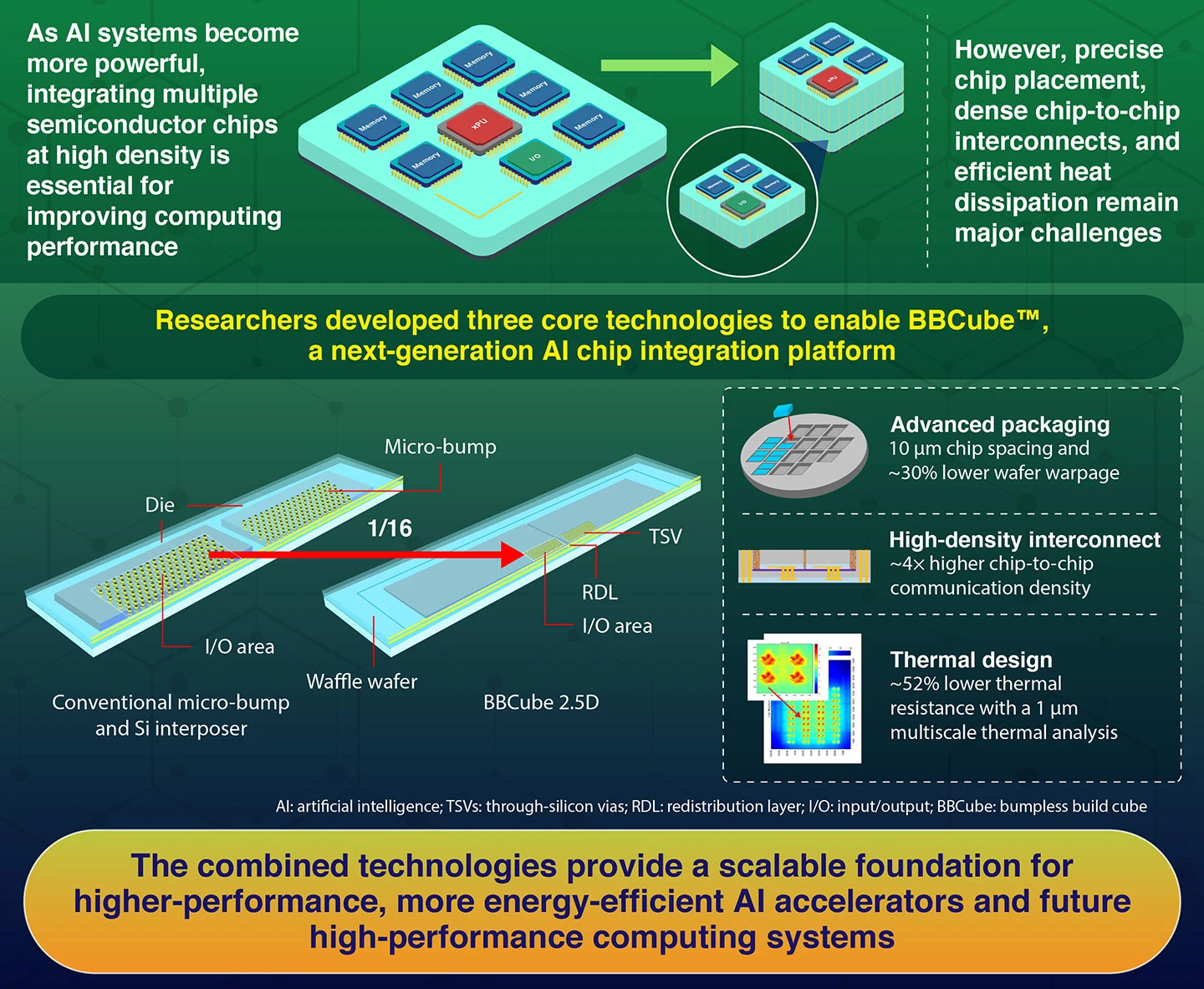
In this context, a research team led by Specially Appointed Project Professor Norio Chujo from the WOW Alliance Heterogeneous and Functional Integration Research Unit, Institute of Integrated Research, Institute of Science Tokyo (Science Tokyo), Japan, together with Researcher Hideki Kitada and Specially Appointed Project Professor Takayuki Oba from the same institute, in collaboration with the WOW Alliance, developed three core technologies to enable BBCubeTM, a next-generation semiconductor integration platform for AI systems. Their innovation was presented at the 2026 IEEE 76th Electronic Components and Technology Conference (ECTC) held in Florida, USA, from May 26 to 29, 2026, and the 2026 IEEE/JSAP Symposium on VLSI Technology and Circuits held in Hawaii, USA, from June 14 to 18, 2026.
“We developed three key technologies required for advanced 2.5D and 3D integration: our proprietary high-density chip-on-wafer technology, bumpless chip interconnection technology, and multiscale thermal analysis technology,” explains Chujo.
Additionally, the team developed a high-density chip interconnection architecture based on the BBCubeTM process. In this process, via last through-silicon vias (TSVs)-tiny vertical electrical pathways formed after the chips are placed-connect the chips without using the metal bumps required in conventional packaging. This bumpless structure allows many more electrical connections to be placed within a limited area.
By combining these fine-pitch interconnections with the highly accurate chip placement described above, which reduces the chip-to-chip spacing to 10 µm, the analysis indicates the potential to provide up to 16 times greater aggregate signal bandwidth within the same interconnection area while maintaining signal quality comparable to that of conventional micro-bump-based designs.
“By placing chips closer together and connecting them without conventional bumps, we can greatly increase the amount of data transferred within a limited area without sacrificing signal quality,” notes Chujo.
Another major obstacle was the heat buildup in densely packed electronics. To tackle this, the researchers used simulations to demonstrate how their waffle wafer structure reduced thermal resistance by approximately 52%. They further developed a multiscale thermal analysis method capable of evaluating heat distribution across an entire chip at 1 μm resolution using 100 million analysis points, making it possible to accurately assess emerging semiconductor designs.
Together, these three technologies form a single efficient platform, advancing next-generation semiconductor systems. By addressing some of the most pressing challenges in AI hardware, BBCubeTM holds the potential to accelerate the development of faster and more energy-efficient systems with compact packaging, efficient connectivity, and effective heat dissipation. As semiconductor devices continue to grow in complexity, further development of such technologies may support more compact chip architectures, helping power the future of AI accelerators and high-performance computing systems.
Reference
- Authors:
- Article 1:
Hideki Kitada1, Yoshiaki Satake1,2, Wataru Doi1,2, Naoko Araki1,3, Hiroyuki Ryoson1,4, Norio Chujo1*, Tatsuya Funaki1,2, Azusa Yagi1,5, Toshiyuki Takasaki1,6, Takashi Yoda1, Tadashi Fukuda1, and Takayuki Ohba1
Article 2:
Norio Chujo1*, Shinji Sugatani1, Koji Sakui1, Masao Taguchi1, Hiroyuki Ryoson1, and Takayuki Ohba1
Article 3:
Hiroyuki Ryoson1, 2, Shinji Sugatani1, and Takayuki Ohba1
- Titles:
- Article 1:
High-Density Chiplet Integration using Face-Down COW Processes with Bumpless Interconnects for Heterogeneous 3D Systems
Article 2:
BBCube 2.5D: A Bumpless 2.5D Integration Technology Enabling High-Density Inter-Chiplet Interconnection Using Waffle-Wafer and Via-Last TSVs
Article 3:
Multiscale Thermal Simulator development for high resolution Hot Spot analysis
- Conference Papers:
- Article 1:
2026 IEEE/JSAP Symposium on VLSI Technology and Circuits (VLSI Technology and Circuits)
Articles 2 and 3:
2026 IEEE 76th Electronic Components and Technology Conference (ECTC)
- DOIs:
- Article 1:
10.1109/VLSITechnologyandCir65830.2026.11577472
Article 2:
Article 3:
- Affiliations:
- Article 1:
1Institute of Science Tokyo, Japan
2Murata Manufacturing Co., Ltd., Japan
3Daicel Corp., Japan
4Dexerials Corp., Japan
5Zacros Corp., Japan
6Panasonic Connect Co., Ltd., Japan
Article 2:
1Institute of Science Tokyo, Japan
Article 3:
1Institute of Science Tokyo, Japan
2Dexerials Corp., Japan